Nfc Card
Batteryless NFC Experiment
I like the idea of business cards that make a point through their existence (like mine), but one problem I’ve had is that of power: these boards need to be powered by USB, or battery. Batteries are bulky or at least take up a lot of surface area. USB can be pretty compact – a 0.8mm board can slot into a USB-C cable, and for those who say “oh yes let’s just plug this unknown circuit board into my laptop”
ahem:
Use a USB wall power source.
But this card still fundamentally requires an external power source of some sort. Wouldn’t it be nice to do away with that entirely?
There are several ways we could achieve this. Solar, for example. Thermal energy. Mechanical energy, although this would require a number of moving parts, whereas solar and thermal can be solid state. What these all share, however, for the application of a business card is that each would provide so little energy per unit time that we need to accumulate the energy, store it, and then expend it in a burst.
That’s actually ok! The speech recognition business card I made is used in a bursty fashion, meaning it’s powered up, used briefly, and spends most of its time being off. Using energy-storing supercapacitors, we can slowly store energy, and then burn it all on the card’s demonstration circuit.
Contents
The Idea
It’s all well and good to have a card with my details on it, but this is of no use to you. What if you could rewrite this to have your details? Contacts are frequently shared with NFC today – Near Field Contact – using RF waves. I want to have a card that one can display their own details on.
In keeping with the theme above, we want this to be batteryless, and therefore consume no passive power; it should only use energy when updating. There are two key usage elements here:
-
Writing to the card with NFC
-
Displaying this new information
For the first, this gives us our power solution. Several NFC chips exist with an energy harvesting option, whereby the energy in the RF waves that contain the signal is also collected and stored, via induction through the NFC coils. Excellent! We feed this into a super capacitor, and with some extra circuitry, can make this fire up a chip when we have enough energy.
For the second, we want this displaying constantly – no use flashing information for 0.1s. Thankfully, eInk displays solve this one. They cost more energy per pixel to change than an OLED display, but crucially cost no energy to continue displaying – only change costs energy.
The usage is then: phone sends information via NFC, and stays within range long enough to transmit enough power. Supercapacitor charges up from this, and when a chip measuring the capacitor hits a limit it opens, and sends a regulated flow of energy through to the main microcontroller. Microcontroller boots in low power mode, reads data from NFC chip, writes to the display (main energy user), and then safely powers down. Display has updated with new information.
Energy considerations
We have to power a microcontroller and the NFC chip long enough to read the message, and then the microcontroller and the eInk display, long enough to update the display. Eyeballing things, since I have no code yet, this should take not more than maybe 100-150ms. Microcontrollers are well-optimised for low-power use cases, so this can be pretty negligible (ditto the NFC chip), so our main concern is the eInk display refresh power usage.
The discussion below on the supercapacitor will detail the energy we can store, and the discussion about the eInk display will detail the energy requirements in greater depth.
The circuit
This circuit has a lot of parts each with a necessary job. I’ll show the flow of energy and information, and go over each part. The basic flow is:
NFC antenna -> NFC chip -> supercap -> load switch -> LDO -> buck-boost/regulator -> microcontroller -> eInk
NFC Antenna and chip
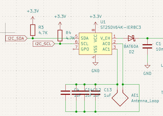
There are two main parts to discuss: U1, the NFC chip, and AE1, the antenna. Everything else is either passive and assistive components, or it actually just got caught in the screenshot and will be discussed next (ahem C1 on the right).
The NFC antenna was designed with a generator script and requires a certain geometry, number of loops, etc to work with the frequency, energy transmission, and guarding against interference. I’ve never done antenna work before, so there’s a lot of uncertainty around this.
Some of the factors are:
- antenna area: more area means more magnetic flux captured, therefore more power harvested
- number of turns: increases induced voltage and inductance, but also increases resistance
- trace width: wider means lower resistance, generally better efficiency
- spacing: affects inductance, parasitic capacitance, and coupling between turns
- inductance of overal antenna: must work with the NFC chip’s internal capacitance to hit resonance (can tune this with components)
Essentially, there’s a certain amount of ‘tuning’ that goes into getting a custom antenna right. Physical characteristics that are baked in, like width, could be countered by capacitors across the antenna, but this whole ordeal likely requires a number of board iterations. One major heuristic I’m working from is to maximise antenna area (given the constraint I’ve placed upon board size of “business card footprint”). We further tune according to the chip’s datasheet, which leads us to …
The ST25DV64K, a standard NFC chip, has 64K of internal flash to store transmitted data – gross overkill as the messages will be small – and an energy harvesting mode. This circuit includes an external power method, so I can do setup work, but the final product will start in energy-harvesting mode. Energy collected by the antenna will be funneled through the rest of the circuit (see below) and when this is enough, will power the VCC and GND rails and the rest of the chip will activate. Then the ST25 can read the NFC data being sent, and communicate this to the microcontroller via I2C in the SDA and SCL lines on the left.
Back to combining this with the antenna, the datasheet for the ST25D specifies that the internal tuning capacitance is $C=28.5pF$. The NFC RF frequency is 13.56MHz, and therefore we need an antenna with an inductance of approximately $L=4.8\mu H$, as per
$f = \frac{1}{2\pi \sqrt{LC}}$
So we’ll need to tune the antenna’s inductance towards that.
Next, there is the question of power draw from the antenna through the chip. The current is a function of the magnetic field strength, and the datasheet provides some tested levels, including ~0.7mA at 3.3v. Using
$E = VCt$
where $E$ is energy, $V$ is voltage, $C$ is current and $t$ is time, the charge time we’ll need to accumulate ~40mJ (see Supercap discussion below for how we get this number) is
$t = \frac{0.04}{3.3\times0.0007}=17s$
Which is a long time to be holding a phone and doing NFC. The datasheet does have different datapoints, for example 4.5mA at 2.57V, and like I said above there’s some experimentation to do with the antenna, but this isn’t looking great.
Supercap
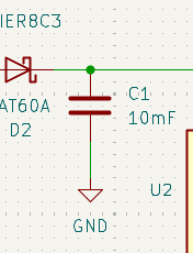
Capacitors are a deep and complex component, but given that we are talking about DC, we can ignore a considerable amount of that. For the usage here, all we need is that a capacitor stores electrical energy. In digital circuits, capacitors typically range from 100 picoFarads to perhaps 5 microFarads, and the use case is smoothing out fluctuations in voltage – since they have energy stored, if the voltage supply dips they can suddenly produce energy to cover that dip, and if it spikes they can absorb the spike.
This capacitor, however, is in the milliFarad range, and that’s enormous. The purpose here, as we know, is to store all the incoming energy from NFC, and then when some future circuit element decides its time, to let this loose and power the rest of the circuit, draining entirely in the process. A battery, of sorts.
If we have 10mF, and discharge from 4v to 2.8v we have
$E = \frac{1}{2}C(V_{hi}^2 – V_{lo}^2) = 0.0408J$
So we have about 40 milliJoules to play with. As mentioned in the Antenna discussion above, this requires considerable charge time.
Voltage Supervisor
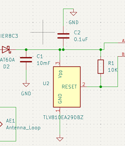
The element in question here is U2, a voltage supervisor. This reads the supercapacitor voltage as it charges and will activate its RESET signal when the voltage is high enough.
Why is this necessary? We could simply let the circuit activate itself when the cap has enough energy stored; after all, a low enough voltage won’t activate the circuit.
However, such a setup would mean that it would activate at the minimum level, and then run out soon after. This allows us to set a higher level, and only activate when we have not just the minimum, but the sufficient energy. Furthermore, it has built-in hysteresis so that brief voltage spikes do not activate the circuit unnecessarily. It will only activate under a consistent reliable load.
Load Switch
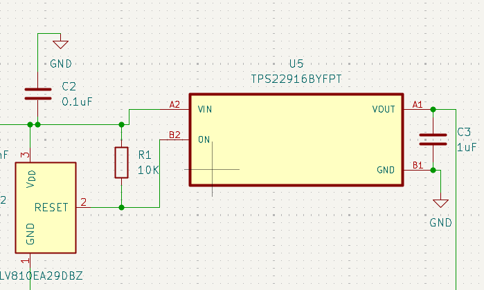
U5 is the load switch, and I include the voltage supervisor so we can see how it feeds into the load switch. A load switch is, at its most basic, a signal-triggered switch. While there is current control, etc, the main feature we care about is this circuit isolation and switching behaviour. When the supervisor detects enough energy to power the circuit for the time we need, it will send a signal to the load switch, which activates and allows current to flow through. The supervisor also manages a stable deactivation, shutting down when the voltage from the cap is too low – this avoids unstable brown-out behaviour. The capacitor C3 on the right helps stabilise the current on the output.
Buck-boost converter
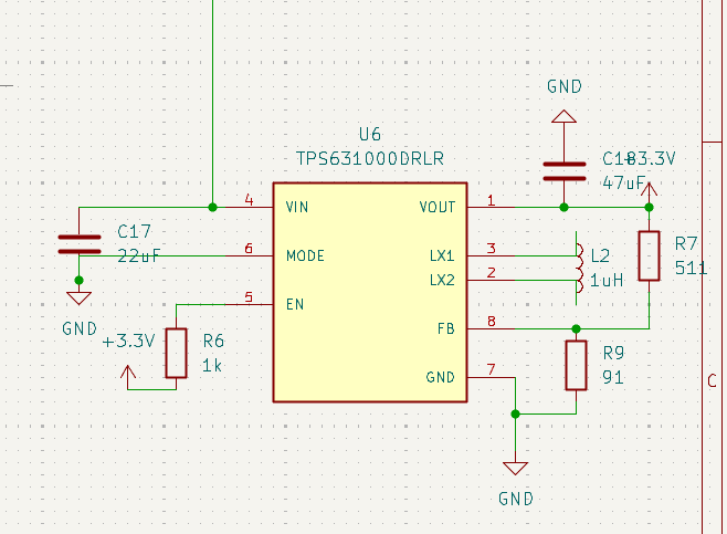
Now that we actually have a power flow, we need to regulate it. I could use a linear 3.3v regulator, but a) those aren’t particularly efficient, and b) if the incoming power line drops below 3.3v, a regulator cannot bring it back up. A buck-boost can. It’ll be more power hungry, but that might be necessary to buy another 50ms or whatever is needed. I originally had a Low Drop Out regulator, to cut off when power got low, but for the initial design I’m going with buck boost – to maintain stable power. This particular module boasts 90% efficiency up to half an amp of throughput, which is far higher than we’re ever going to go.
That’s power sorted!
Microcontroller
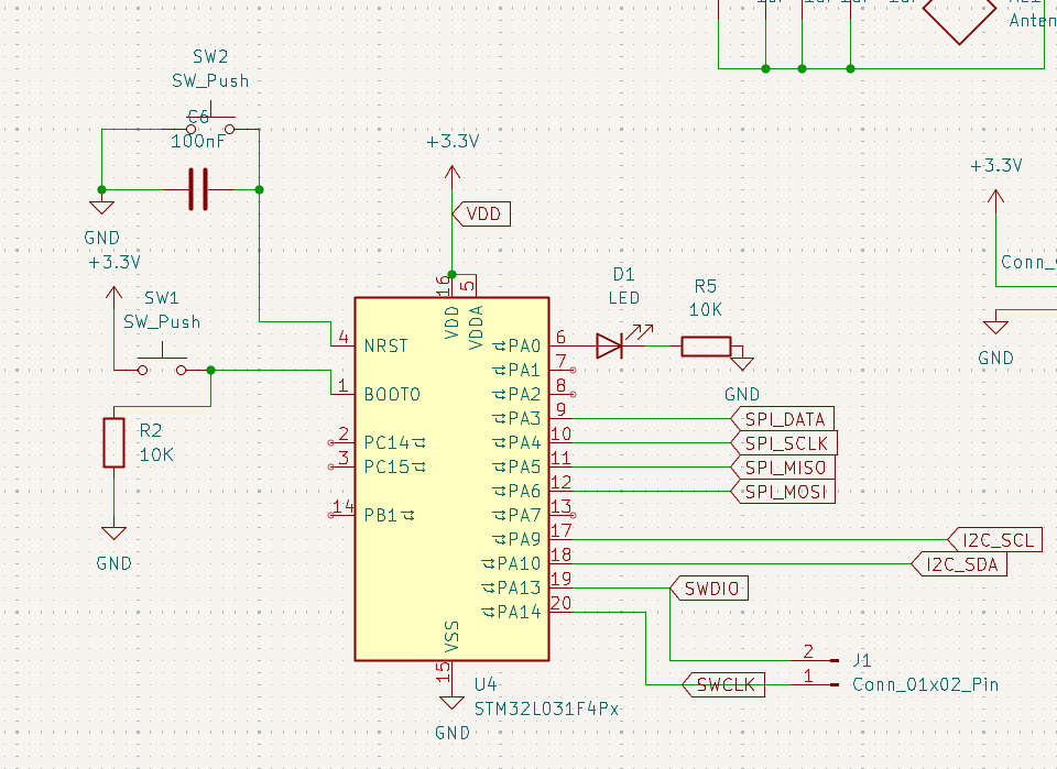
The microcontroller assumes a steady power for the duration of the program necessary. For prototyping, I’m using an external power source anyway, that won’t run out, so no stress there. For actual runtime … this is where some level of experimentation comes in. I’ve run the numbers, and I think it will last.
I’m using the STM32L031 processor – a 32-bit chip designed for low power use cases. Once everything is powered, the intended program is, on a high level:
-
using I2C protocol (pints 17 and 18, lower right), request the NFC message from the ST25D chip (which, being stably powered itself, will have received)
-
Using SPI protocol (pins 9, 10, 11, 12, right middle), and a graphics library, write the text of this message to the eInk display
-
Power down into sleep mode gracefully (honestly, this isn’t strictly necessary)
There is an LED on pin 6 for testing – an LED can be pretty low power, and if I can get it to flash in a certain way, that can indicate reaching a certain part of the program for debugging purposes.
The rest of the circuitry here is for programming mode or reset mode (the switches on the left).
As for power usage, this draws ~2.4mA at 32MHz (that is, we could boost it up to a higher processing frequency … but simply don’t need to. At 50-150ms, we’re drawing negligible current). This is negligible next to the eInk display, so we’ll ignore it. If you want the actual numbers, energy is voltage times current times time:
$E = V \times C \times t = 3.3v \times 0.0024 \times 0.15 = 1.1mJ$
The eInk display
This is not actually part of the initial design! I’ve set some breakout pins for the communication and power, and will hold the screen externally for now.
Tp update the Waveshare 1.54” eInk display, the datasheet reports a maximum of 8 mAs - 8 milliamp-seconds. Energy is voltage times charge, where charge is current by time, we get
$E = V \times C \times 1s$
$= 3.3v \times 0.008 \times 1$
$= 26.4mJ$
This is the maximum energy required for a full screen update. We can optimise this by using a smaller display, or by just partially updating this display. If we update a fifth of the screen, we can use ~ a fifth the power, and achieve ~5mJ draw from the display.
From above, we can store about 40mJ of energy. We’re well within budget drawing 25, but I like to live on the safe side. This also means, if we can reduce energy budget, that we could also not charge for as long. Recall that charging to 40mJ could take ~17 seconds. If we charge to 5mJ + 1.1mJ, we’re down to ~2.6s.
PCB layout
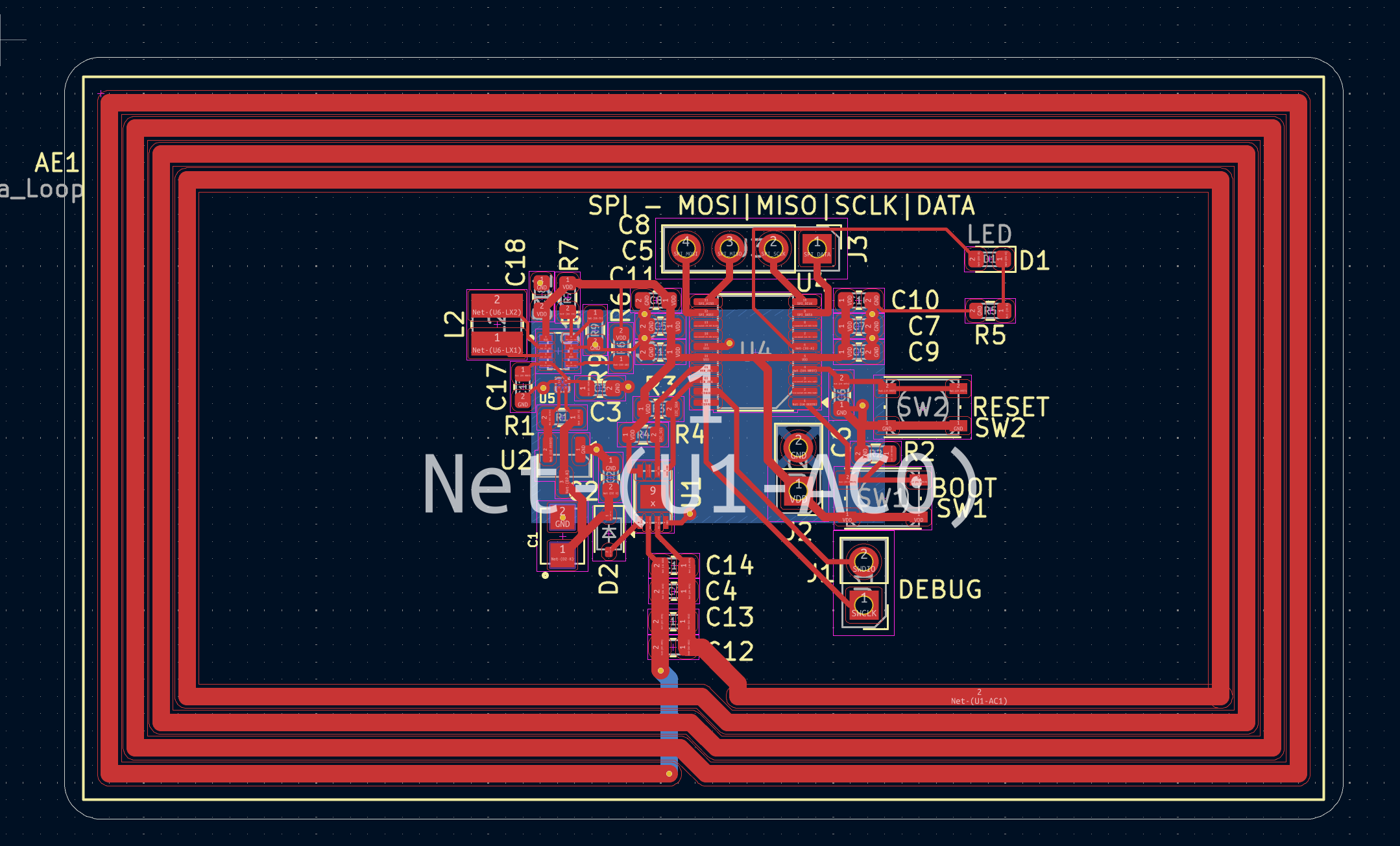
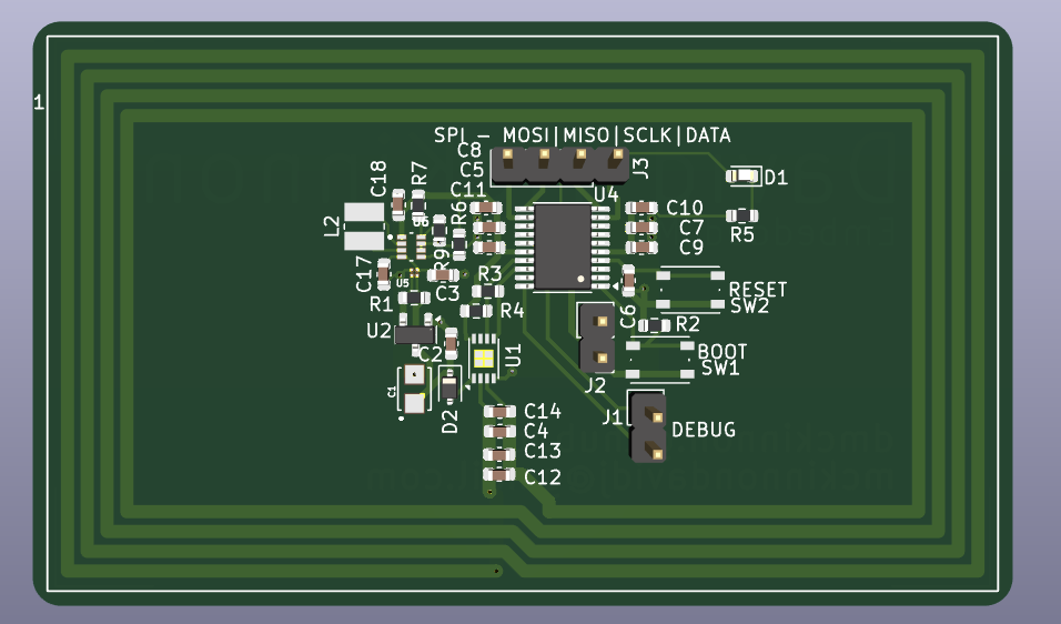
It’s tight! Circuit files here if you’re interested in perusing closer.
There’s a major potential problem here. NFC is a radio-frequency electromagnetic signal, which induces current in anything metal. The small metal legs of compnents aren’t much, but there’s a lot of them, they’re connected by traces, and NFC requires precision. What’s even more alarming is the GND plane on the back layer, seen as the centre blue rectangle in the upper picture.
Ground planes are a useful circuit feature for cleaning up noise and reducing stray capacitance, so we want some level of GND plane, BUT … this also is ripe for allowing an opposing magnetic field that would affect the NFC signal. So there’s a tension between making this as small as possible, but also having it still exist. Something to experiment with.
“Couldn’t the NFC antenna be off to one side, with no components inside?” Yes, this is entirely possible.
However, this affects the energy we can capture - as discussed in the antenna section, antenna area is proportional to power captured, and I want to maximise this per unit time.
Fabrication
I can hum and haw and calculate away until the cows come home – or until I purchase some cows – but all of that is meaningless if I don’t actually try. To get it fabricated, I’m using PCBWay. I’ve used them before, it’s a really easy and affordable service and I’ve had a great experience.
To get a quote, you give basic info like dimensions, # of layers, colour (we’re going blue for this one), and you get a ballpark price then and there:

After exporting and uploading all necessary files from KiCad (which is really easy and they document how to do it), one of their technicians will take a look – on previous projects I’ve had some back and forth about some parameters or errors that I’m glad they found.
Once all that is sorted out, it gets fabricated and shipped, and a ride across the Pacific later (for me) it’s at your door. For parts I go Mouser or Digikey, and of course if you don’t want to solder parts yourself PCBWay also has the option of doing this for you as well.