Analog Computers
Analog Computers
Contents
Back in the Dark Ages, before general purpose computers existed, if you wanted a program that would compute a particular equation for arbitrary inputs you had to make a one-off device. Today’s digital computing allows for general mathematics and logic - a program can be written for any particular math you might want to do, and rerun on the same hardware. Such is the blessing of digital computing. Without this … Analog Computers were used. Let’s say you want to know the trajectory of a projectile given some initial conditions, drag coefficients, etc. You want to know where it might land, given the angle it was fired at, the initial speed, and so on. This is a set of differential equations. You could work it out on paper … but then what if you have a series of inputs, and you need it for all of them? That’s a lot of work. And let’s say you need the answers in a minute. Well, that’s not helpful. So, barring access to a digital computer and a program that can do this as it hasn’t been invented yet, you turn to Analog Computing, and build an electronic circuit designed to solve this exact mathematical problem (but only this mathematical problem), for any reasonable inputs and initial conditions.
Such circuits were in use earlier in the 1900s, and once digital computing came about they were largely put aside; programs are more versatile, more general purpose, and better in almost every way for usability. So how does this work? My aim was to construct such a circuit for the Lorentz Attractor differential equations as an exercise in understanding this. I did go from a template, but there’s enough faffery involved that I ended up learning a lot too. For reference, the Lorentz Attractor equations are
$\frac{dx}{dt}=\sigma(y-x)$
$\frac{dy}{dt}=-xz+rx-y$
$\frac{dz}{dt}=xy-bz$
But it’s not particular important to know this now. The main point is I tried to make “a circuit that did some math”.
First, we need to go over the basic building blocks of “mathematical circuits”, for want of a better phrase, and then we’ll build up to getting the whole circuit together.
Op-Amps
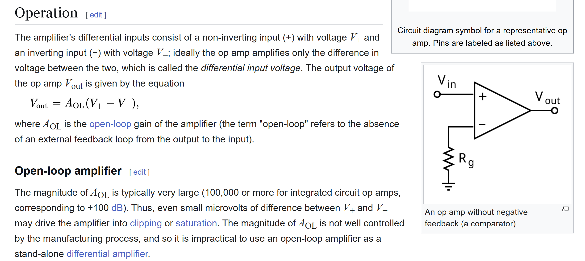
Op-Amps, or operational amplifiers, are a key circuit element here. I misunderstood them originally and assumed they exist to, well, amplify a signal. They have two inputs, and one output. The output is the difference of the inputs, amplified by some factor. So if you want one signal amplified, connect the other to ground (0v), and then that should be amplified on the output, and you just choose a unit with the amplification factor you want. Right?
No.
Their usage is a lot more arcane than this.
The actual functionality has been written about extensively elsewhere, and I’m going to repeat a lot of it writ more simply, so if you already know a lot of this then feel free to skip to the next section.
Firstly, let’s go over how they work - feel free to skip this, but it should help with later - and then I’ll go over how they are used in Analog Computers. We’re going to get to my actual circuit design eventually.
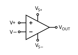
The following is a circuit diagram of an op-amp, with output $V_{out}$, and the two inputs $V_+$ and $V_-$. The other voltage lines ($V_{S_+}$ and $V_{S_-}$) are to power the whole thing, and these also provide upper and lower limits to the output voltage. I’ll ignore these in future diagrams, as power rails are assumed.
The op-amp equation is
$V_{out} = A(V_+ - V_-)$
So, as stated above, the output is the amplified difference of inputs.
Typically $A$ is something on the order of 100 000. This is where my initial confusion lay - I assumed it would be 2 or 3, and maybe you’d buy an extreme one that had a factor of 10 or you’d chain a few to get a bigger one … no. It’s actually meant to be infinite gain, in theory.
I don’t understand why - what use is something that amplifies a tiny difference infinitely?
There’s a missing piece though - the feedback loop. If we connect $V_-$ to $V_{out}$, then $V_{out}$ will amplify the difference between $V_+$ and … $V_{out}$. So if $V_{out}$ drops below $V_+$, $V_{out}$ is amplified to create a larger positive signal … bringing it back up. If $V_{out}$ goes above $V_+$, this creates a negative signal, bringing it back down. The stable equilibrium, which analog circuits like, is the state where $V_-=V_+$, and $V_{out}$ produces a steady-state signal. This is called the virtual short: $V_+=V_-$. Not quite a law, but just the stable steady state. Note that because the gain is “infinite”, even tiny differences are amplified.
We can now exploit this. Consider this connection:
The Voltage Follower
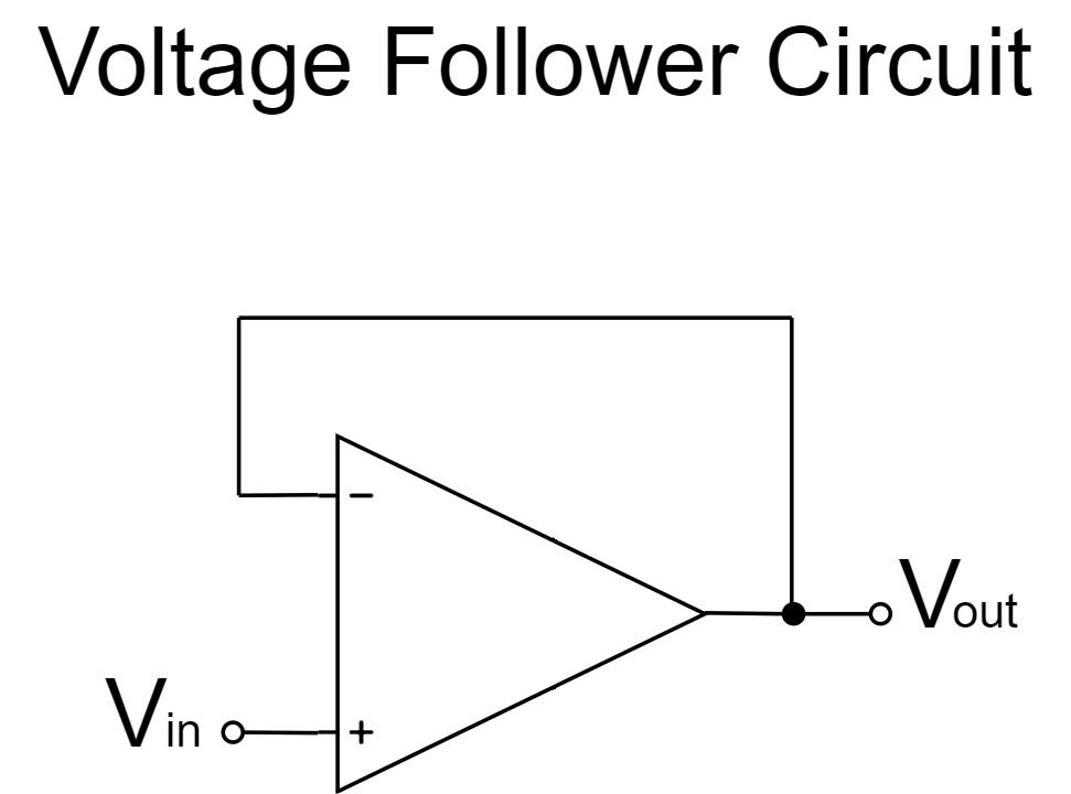
Now we have $V_{out} = V_-$, and $V_+ = V_{in}$. The op-amp will drive $V_{out}$ to be the amplified difference of $V_+$ and $V_-$, as per $V_{out} = A(V_+ - V_-)$. We can rewrite this, with our new information:
$V_{out} = A(V_{in} - V_{out})$
Expanding and rearranging,
$(1+A)V_{out} = AV_{in}$
and then
$V_{out} = (\frac{A}{1+A})V_{in}$
Given that $A$ is ~infinite, but in practice 100 000 or so, this is practically 1 and therefore we have a “voltage follower”. This means that $V_{out}$ is driven to whatever $V_{in}$ is. Why does this matter? We could simply just continue a wire from $V_{in}$ … what does this buy us? Well, apart from demonstrating the feedback mechanism of op-amps, this circuit “isolates” $V_{out}$ whilst allowing it to copy $V_{in}$. That is, $V_{in}$ might be a low-current signal and $V_{out}$ might require a higher current than $V_{in}$ can deliver, but because the op-amp is externally powered, $V_{out}$ can draw far more current and stay the same voltage. Anyway, this is a digression. We don’t necessarily need this for the mathematics.
This basic feedback mechanism and mathematical trick, relying on the op-amp to drive $V_{out}$ however necessary to produce the requisite voltage, can then be exploited to create several more useful circuits:
The scaler
(or amplifier, but now that’s become an overloaded term):
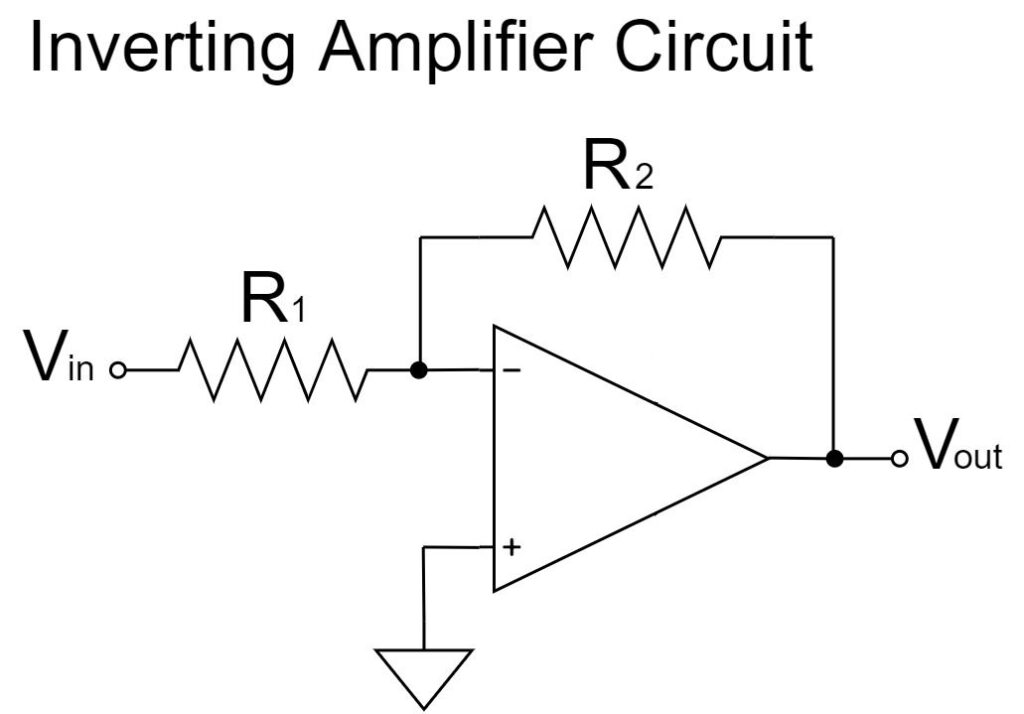
Consider the inverting scaler first. $V_+ = 0v$, and by the virtual short steady state $V_- = 0v$. Therefore all current from $V_{in}$ must flow through the feedback resistor, thanks to Kirchoff’s Current Law. So we have, at the $V_-$ node,
$\frac{Vin}{R_1} = \frac{(0-V_{out})}{R_2}$
Solving for $V_{out}$ gives $V_{out} = \frac{-R_2}{R_1}V_{in}$.
By choosing $R_2$ and $R_1$, we can scale the input voltage by various factors, eg. $R_2 = 2*R_1$ to double it.
The non-inverting follows with only a little more working:
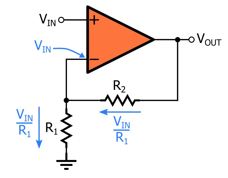
$\frac{V_{in}-0}{R_1} = \frac{V_{out}-V_{in}}{R_2}$
$V_{out} = R_2(\frac{1}{R_2} + \frac{1}{R_1})V_{in}$
So $V_{out} = (1+\frac{R2}{R1})V_{in}$
Note that this can only scale greater than one, but you can always just chain two inverting scalers to achieve fractional scaling
The Inverting Summer
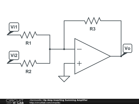
This follows from Kirchoff’s Current Law, the fact that currents add together - the current at $V_-$ is the sum of the currents from each of $V_1$ and $V_2$ - therefore $\frac{-V_{out}}{R_3} = \frac{V_1}{R_1} + \frac{V_2}{R_2}$, so we get $V_{out} = \frac{-1}{R_3} (V_1R_1+V_2R_2)$ By setting $R_2 = R_1 = R_3$, we can cancel out the resistance scale factors, and $V_{out} = -(V_1+V2)$ This can be made to do general weighted linear equations - a dot product with static weights, if you will. Since Kirchoff’s Current Law tells us that all the currents at the left node are summed, we can have as many signals as we want, with resistances, leading into this. The resistances can be different for each input voltage. These resistances form the static weights, the voltages are summed, and then the result is scaled by the feedback resistor to get $V_{out} = \frac{-1}{R_{feedback}} (R_1V_1 + R_2V_2 … )$
The Subtractor
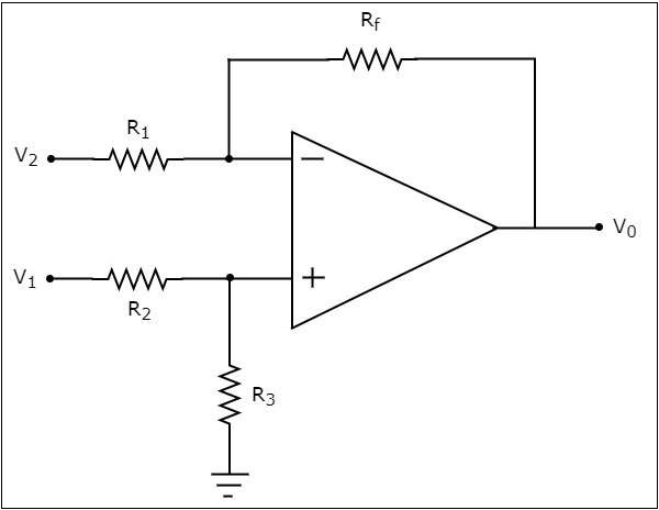
This is slightly more complicated. Given we don’t care about amplifying, we just want to subtract, let’s say that all resistors are just some value $R$.
As $V_- = V_+$, and $V_+=\frac{R}{R+R}V_1=\frac{V_1}{2}$, we have
$\frac{V_2-V_-}{R} = \frac{V_- -V_o}{R}$
$V_-(\frac{2}{R})=\frac{V_2}{R}+\frac{V_o}{R}$
Substituting,
$\frac{V_1}{2}\frac{2}{R} - \frac{V_2}{R}= \frac{V_o}{R}$
And therefore
$V_{o}=V_1-V_2$
This can be made more complicated, into a more generalised linear equation with different resistor values.
There’s a few more blocks, but the point hopefully is clear by now - we can use these circuit elements - op-amps and resistors - to do some simple mathematics on voltages. We could create, for example, a circuit that produces an output voltage y where $y = 2x + 3$. You then just need to have a dial that lets you set $x$, and then you measure $y$. Simple, easy to do on paper, but if you needed to produces results quickly and could set and read voltages quickly, and also digital computing had not been invented, then such a circuit could be useful. Still, probably too simple and contrived to be worthwhile.
Earlier I mentioned I was attempting a differential equation. These contain derivatives and integrals. How do we perform that with op-amps?
The Integrator
Integrals are just adding a lot of small bits up, and we have adders (summers), but a major drawback of analog computing is that there is no storage. For this, we need a time-based element.
Enter the capacitor. Capacitors work in a much more nuanced and complex way than I’m about to describe, but the following should be all that’s necessary to know for the topic at hand. A capacitor has two plates, and if there is a voltage difference across them then one side charges up to equalise the voltage, neutralising the difference. This can then quickly discharge if the voltage across suddenly changes due to external factors.
So if we connect a capacitor across the op-amp feedback loop:
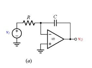
Then as $V_{in}$ changes, $V_{out}$ is driven to be the same as $V_{in}$ (so that $V_+$ is 0). But capacitors introduce some time delay - they must charge up to neutralise a voltage difference, it’s not immediate. I’ll not go into the derivation here, but we know that the voltage across the plates of a capacitor is equal to the charge on the capacitor, divided by the specific parameters called capacitance, which is really just a factor derived from physical construction (materials, dimensions, etc). $V_{in}$ changes, and the charge therefore changes. If $V_cap$ is the voltage across the capacitor, then
$V_{cap} = \frac{Q}{C}$
$V_{cap} = V_- -V_{out}$,
but $V_-$ is 0 due to the feedback loop, so
$V_{cap} = -V_{out}$
The rate of change of $V_{out}$ over time is proportional to the rate of change of charge over time. But rate of change of charge over time is current, and the current flowing in is $I_{in} = \frac{V_{in}}{R_{in}}$
So $I = \frac{dQ}{dt} = C\frac{dV_{out}}{dt}$
Solving for $V_{out}$, we get
$V_{out} = \frac{1}{C} \int I_{in} \,dt$
and $I_{in} = V_{in}/R_{in}$, so
$V_{out} = \frac{1}{RC} \int V_{in} \,dt$
… and thus we can compute the integral of $V_in$ over time.
This might still be confusing, so here’s an exmaple with a periodic signal that might make it clearer:
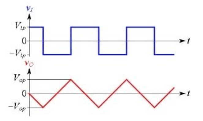
Where the input voltage over time is blue, and the output red. As $V_{in}$ switches, the output signal starts accumulating, proportional to the area under the signal of $V_{in}$. $V_{in}$ then switches again, and $V_{out}$ starts dropping, as the “area under the signal” decreases. This occurs in a sliding window fashion, meaning the integral value, the value of $V_{out}$, really only holds true for a moving time window of $V_{in}$. If $V_{in}$ was a constant value, say, 1v, then $V_{out}$ would simply keep increasing until it saturated. If $V_{in}$ was then changed to 0v, $V_{out}$ would decrease down to 0.
This holds for more complex input signals too. Sines become cosines, and so on.
So we can compute integrals. Can we invert this?
The Differentiator
Instead of connecting the capacitor in the feedback loop, what if we put it before the feedback loop?
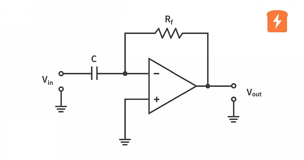
In this case, we have the situation where $V_{cap} = V_{in} - V_-$ (and $V_- = 0$),
$I = \frac{dQ}{dt}= C\frac{dV_{in}}{dt}$.
By KCL, $I = \frac{V_{out}}{R_f}$, so now
$C\frac{dV_{in}}{dt} = \frac{V_{out}}{R_f}$,
and we can rearrange this and see that $V_{out}$ is now proportional to the derivative of Vin over time, instead of the integral! A scaling factor of $RC$ falls out, and we’ll see that explained in the next section.
From the capacitor’s perspective, as it charges under a changing voltage, a current flows across it, proportional to the rate of change of voltage. As voltage changes more intensely, more current flows - since the capacitor reacts and charges quicker. If voltage changes slowly, the capacitor charges or discharges slower (since the difference in potential energy across it is lower) and therefore less current flows. The current flowing through determines the output voltage.
Again, this is demonstrated nicely in some diagrams:
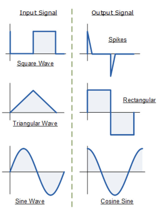
If we put in a triangular wave, we see a square wave out, a square wave produces impulses, sines become cosines, etc.
One final aside about both integrators and differentiators: as capacitors are frequency-dependent circuit elements, these mathematical blocks only work within certain frequency bands. At 0Hz, so DC, capacitors are open-circuits and no current flows. At high frequencies, like the MHz range, we get … unstable behaviours, and we need a different circuit to stabilise these. You also get other factors coming into play. But for kHz, we’re fine and the above equations hold.
Alright! We now have calculus!
The Lorentz Attractor
Back to the original idea: I mentioned earlier I was attempting a circuit with Lorentz attractor equations. These differential equations are:
$\frac{dx}{dt}=\sigma(y-x)$
$\frac{dy}{dt}=-xz+rx-y$
$\frac{dz}{dt}=xy-bz$
This creates a pretty 3D plot in $x$, $y$, and $z$ that looks something like
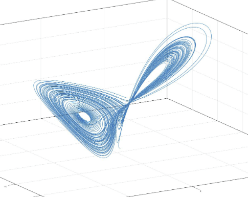
This is with $\sigma=10$, $b=\frac{8}{3}$, and $r=28$. Why? Because … if you pick those, it looks nice. Pick different, and it looks different.
We have derivatives, multiplication by constants, some basic arithmetic … we can do all this! Since we plot $x$, $y$, and $z$, we’ll feed the terms for the derivatives into an integrating op-amp setup, and that will give us … well, an inverted, signal, but an inverting amplifier can correct that. Let’s take a look at constructing an analog circuit that computes this equation - an analog computer, if you will.
Let’s start with the X equation. $\frac{dx}{dt}=\sigma(y-x)$
(We’ve chosen $\sigma=10$ but I’ll get into that below)
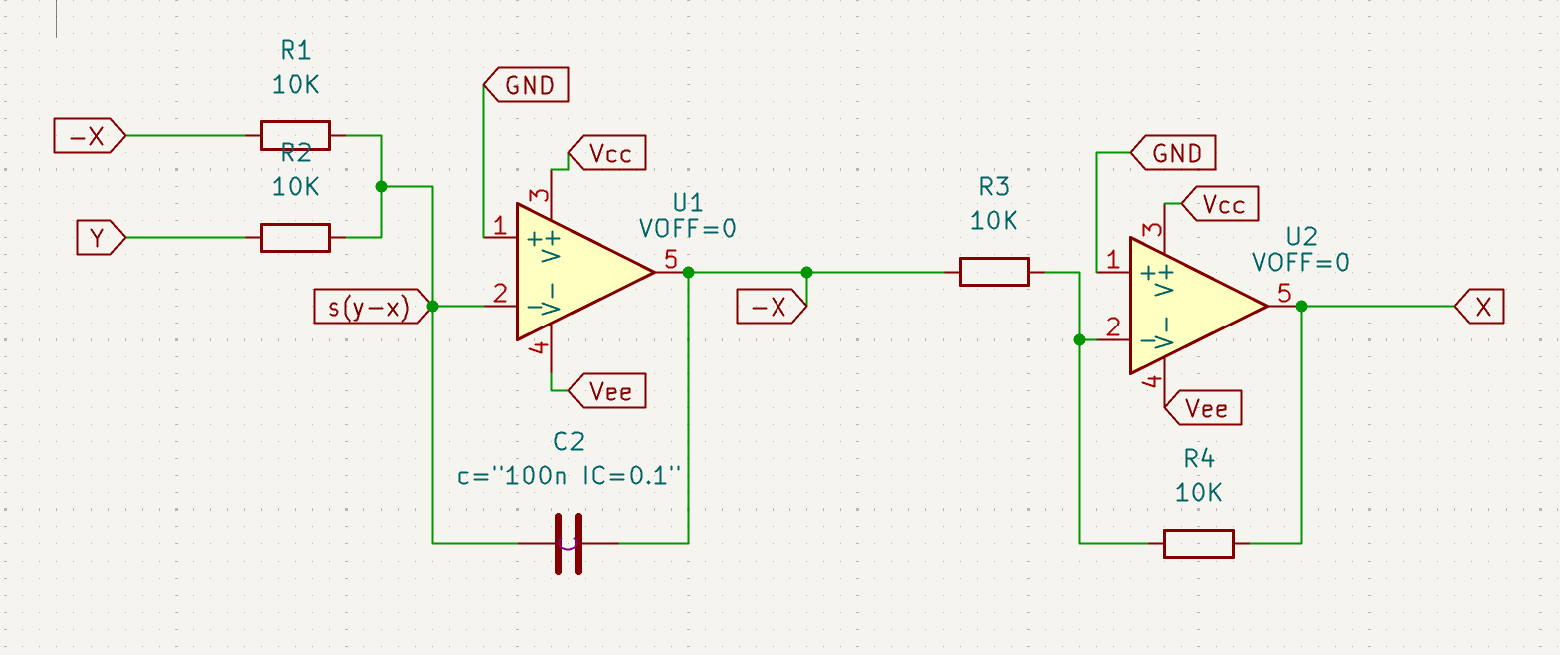
Let’s read this from left to right. On the left, labels for the $-X$ signal and the $Y$ signal. The currents for these signals sum at the label $s(y-x)$, where I’m using $s=\sigma$, as per Kirchoff’s Current Law. This feeds into an integrating op-amp at $V_-$. Using the working from above, and using $V_{out}=label(-X)$,
$V_{out} = \frac{1}{RC} \int V_{in} \,dt$
Therefore
$-X = V_{out} = \frac{1}{RC} \int Y - X \,dt$
Where $C$ is the capacitance of C2 in the diagram, and $R$ is the input resistance for $V_-$ - we’ll tune this to get the $\sigma$ that we want.
The op-amp to the right is a basic inverting amplifier with scale factor 1, and as we feed in $-X$, the output is $X$. This is the signal we measure for plotting purposes, and also to pass into the other differential equations.
Before going over $Y$ and $Z$, let’s discuss the $RC$ parameter and the part it has to play.
We’ve chosen $\sigma$ to be 10, so we want to scale $(y-x)$ by 10. How do we do that in an integral?
Assume some general value for $R$, and pick the integrator input resistors as $\frac{1}{10}R$. Then
$-X = \frac{1}{\frac{1}{10}RC} \int Y - X \,dt$
Since integrals are linear, and since we could have two separate intgegrators and sum them afterwards, we can do
$-X = \frac{1}{RC} \int \frac{1}{10}Y\,dt + \frac{1}{RC}\int -\frac{1}{10} X \,dt$
Recombining,
$-X = \frac{1}{RC} \int 10(Y – X) \,dt$
And then differentiate wrt $t$ both sides,
$\frac{dx}{dt} = \frac{1}{RC}10(y-x)$
Alright so we’ve scaled to what we want. This can be repeated across all three equations, and we see a factor of $\frac{1}{RC}$ emerge, scaling everything down. This has several implications:
- From the plot above, we know the absolute limits of $X, Y, Z$ in these equations, and maybe we don’t want to use voltage that high. Eg. $Z$ might reach 50V! This term, and the parts it uses, can help us scale things down to manageable levels. For example, we could choose $R$ and $C$ such that the outputs never exceed, say, +/- 5v. Perfectly manageable.
- We can derive all the other resistor values from this. Set $R=100k\Omega$ - a pretty standard resistor size – and then the resistors for the $X$ equation above become $10k\Omega$ each (as they are $\frac{1}{10}R$). We can do similar to get factors of $28$ and $\frac{8}{3}$ in the other equations, as you’ll see. $C$ also acts as a time component. The larger we choose the capacitance, the slower the whole circuit oscillates. Want this to oscillate in the MHz range? A really small $C$, which scales the circuit differently. I wanted to sample in the kHz range, which means I increased the capacitance to slow everything down.
Hopefully all that makes sense! If not, just read it as “we’re choosing values relative to a baseline, that determines the maximum voltage levels, and there’s just some magical scale parameter there”.
Onto the equation for Y!
$\frac{dy}{dt}=-xz+28x-y$
(I’ve now subbed in $r=28$)
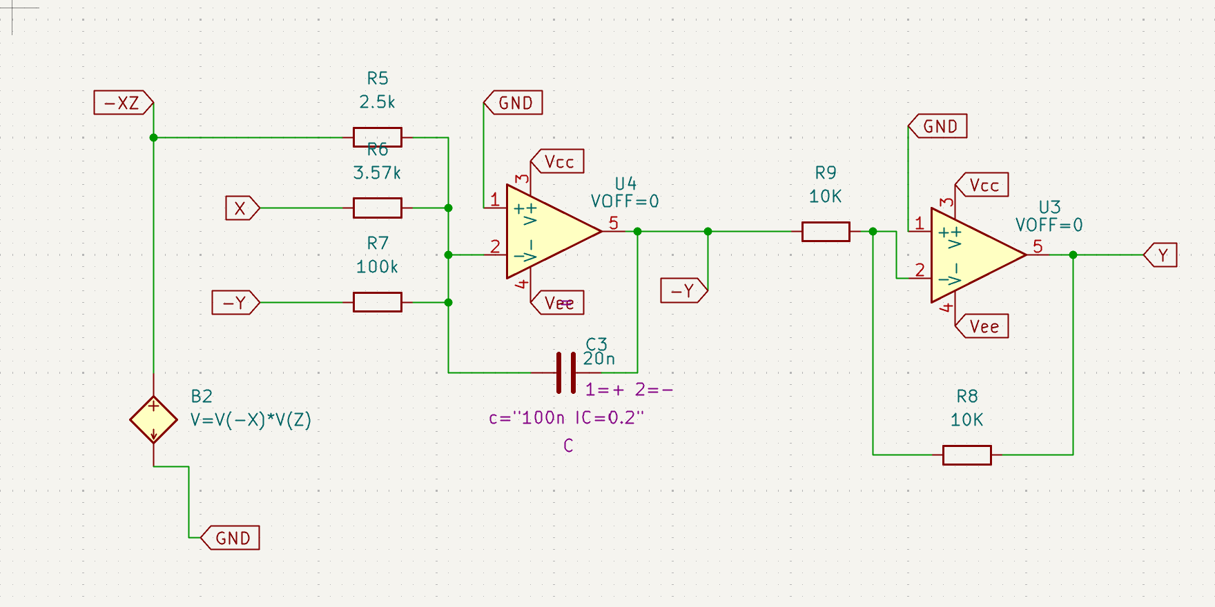
On the left, we have $-XZ$, $+X$ (from the $X$ circuit), and $-Y$, and each term is scaled by a resistor. As $-Y$ has no coefficient, it gets scaled by the “default” value, $R=100k\Omega$. We want $28X$, and $100/28 = 3.57$ (remember, the scale factor is $\frac{1}{\frac{1}{28}RC}=\frac{28}{RC}$, which is why here we divide by 28). I’m scaling $-XZ$ by an extra factor. I want to scale the whole circuit down to an acceptable level, but any global scale factor on $X, Y, Z$ gets squared through the multiplier stage, so I need a “fudge factor” to undo that square.
Then we sum the signal and pass it through the integrator - $C$ is the same here, I use the same value capacitors globally. To do otherwise would … change the frequencies for different equations and produce something I don’t want. We get the $-Y$ signal from the integrator, invert with a scale 1 to produce $Y$.
Finally, Z:
$\frac{dz}{dt}=xy-\frac{8}{3}z$
(using $b=\frac{8}{3}$)
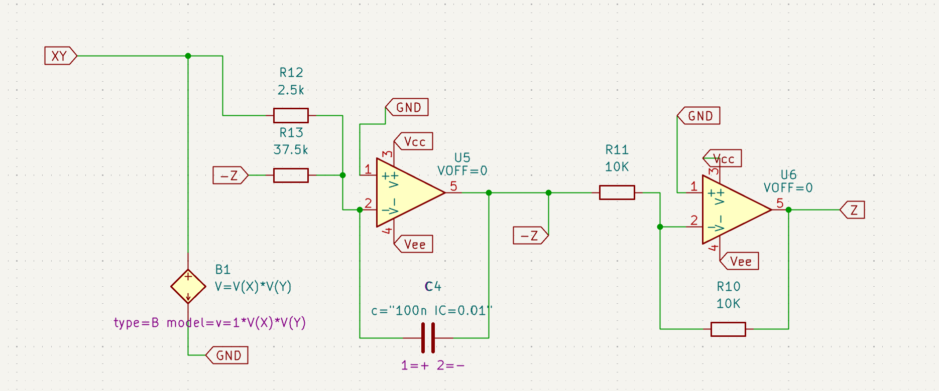
By now this should be recognisable. $-Z$ is a feedback signal from the integrator result, and it is appropriately scaled, then added to $XY$. As $XY$ is a multiplied signal, we have the special “anti-square fudge factor” from above. The scale parameter on $-Z$ is $\frac{100}{\frac{8}{3}}$. These are integrated to form the future $-Z$ signal, which is then inverted by an inverting amplifier of scale 1 to produce $+Z$.
Here’s the complete circuit:
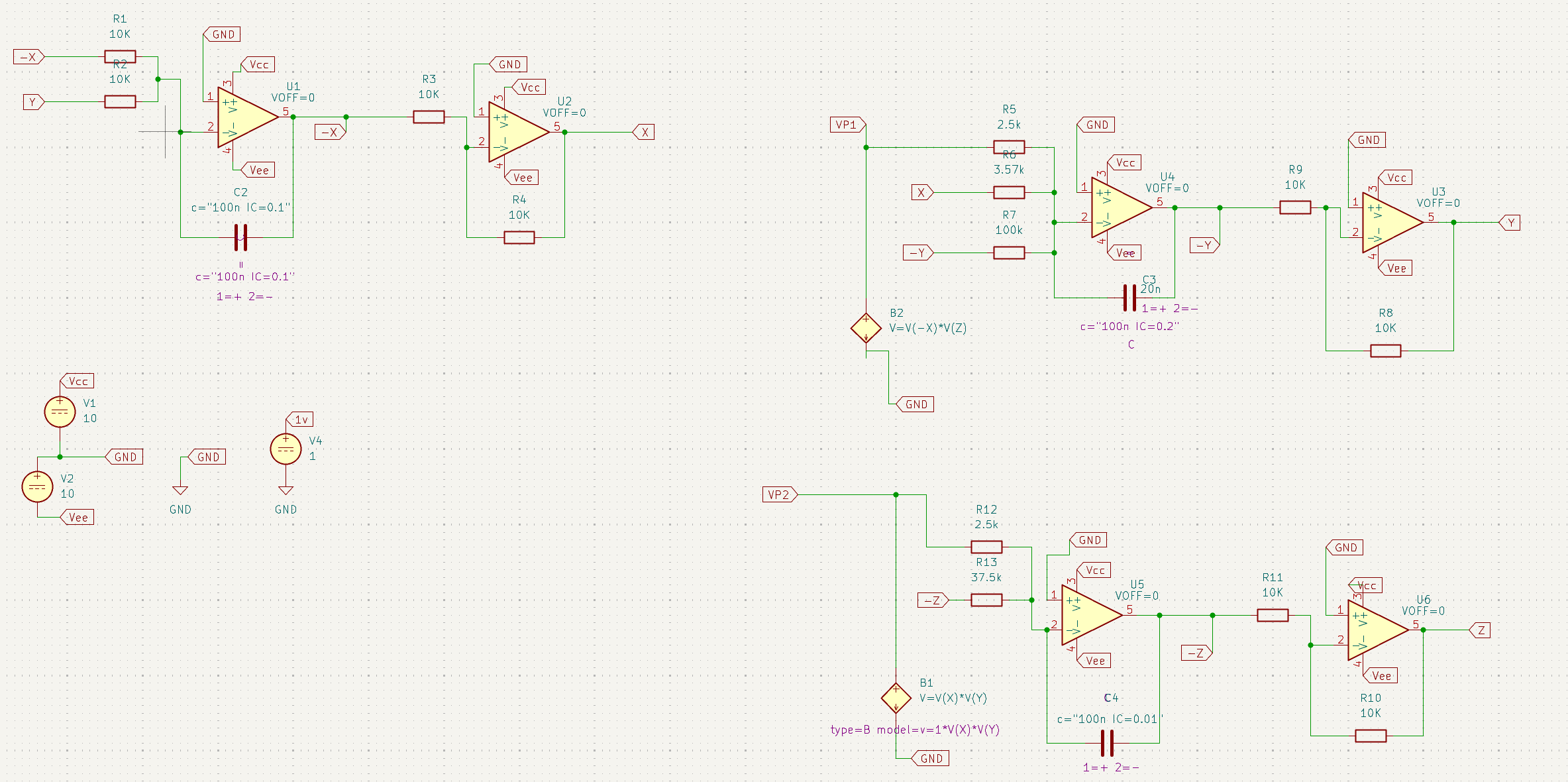
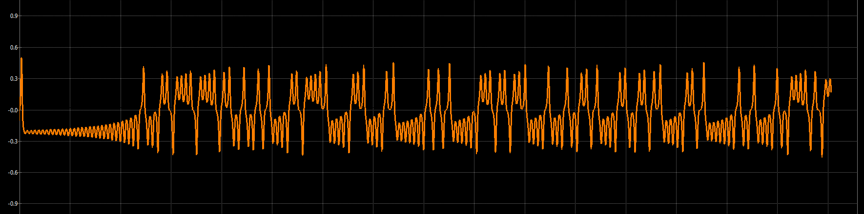
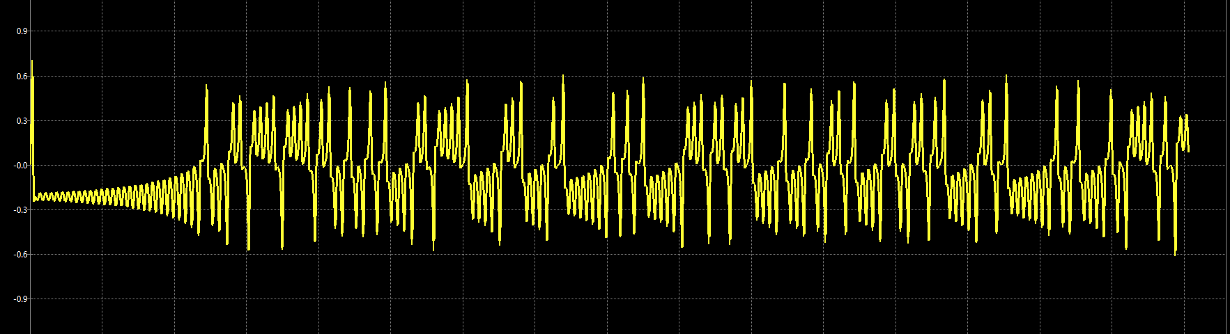
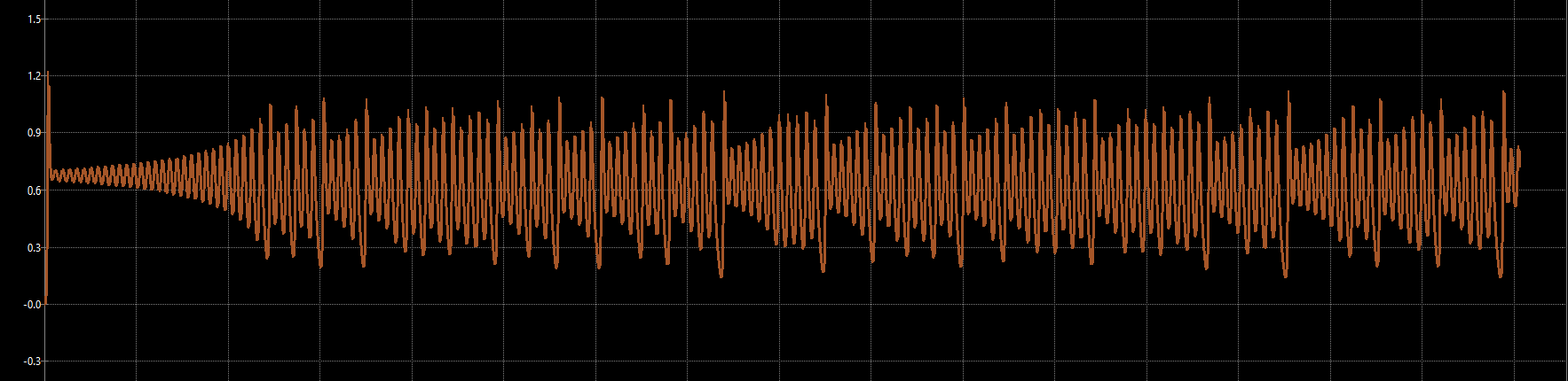
And here’s the waveforms for X, Y, and Z, respectively, measured from my simulation:
Here’s the ground truth waveforms we expect for X, Y, and Z respectively, plotted against time:
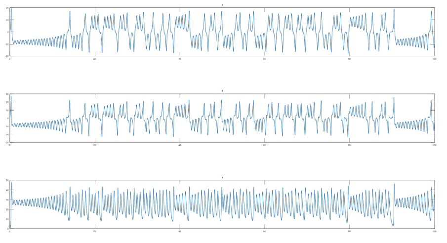
It works!
So we have it simulated. Can I physically build it?
Multipliers
Well, I glossed over something above -how do we get XY and -XZ? These are multiplication of two varying signals, we can’t do this like multiplying by a constant! How do we do this? Above,I’m solving this problem with a simulated voltage source that I can set to be a function of signals:
And we can see that this works. But I can’t just buy a magical chip that does this … Oh wait. I can:
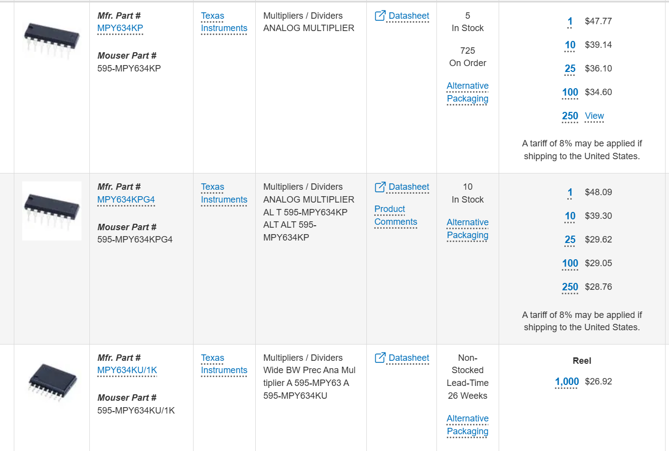
Oh, those are expensive. Can I design my own?
The Transconductance Multiplier
Googling a bit, I found a solution: the transconductance amplifier. One basic use for a transconductance amplifier is a “voltage controlled amplifier”. Where an op-amp amplifies by a factor controlled by a (typically) static resistance, we can used a varying voltage here to amplify another signal. This sounds an awful lot like we are scaling one signal based on another, which must involve multiplication. Checking the datasheet we see:
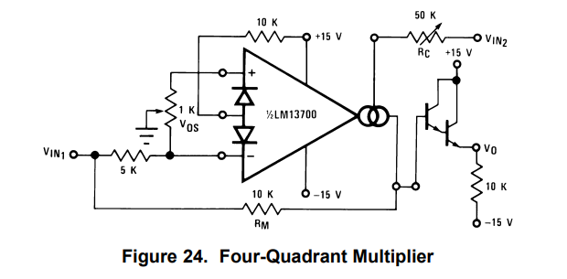
Aha! A multiplier! And the following explanation, accompanying this diagram

That may be a bit dense, but the point is that we now know how the input terms relate to the output, and what constant factors we need to control. I could do a whole write up on multipliers, or indeed just this investigation. I built just this circuit in KiCad and simulated a few input signals. Long story short … it was confusing and did not give me stable results. For some constant signals I got expected results, but for some time varying signals, one would dominate over the other. The resultant wave would be saturated towards one of the inputs, or the expected output would be in the mV-amplitude scale, which would be annoying for the main circuit. I wish I understood why … but this is a less important rabbit hole, and I was struggling to get good answers. So I put this aside.
The Log-Antilog Multiplier
Nonlinear Analog Circuits is a great and specific textbook, and has a chapter on multipliers. It mentions transconductance amplifiers as multipliers, but from first principles rather than from a prebuilt chip. It discusses pulse modulation multipliers. Finally, it discusses log-antilog multiplers:
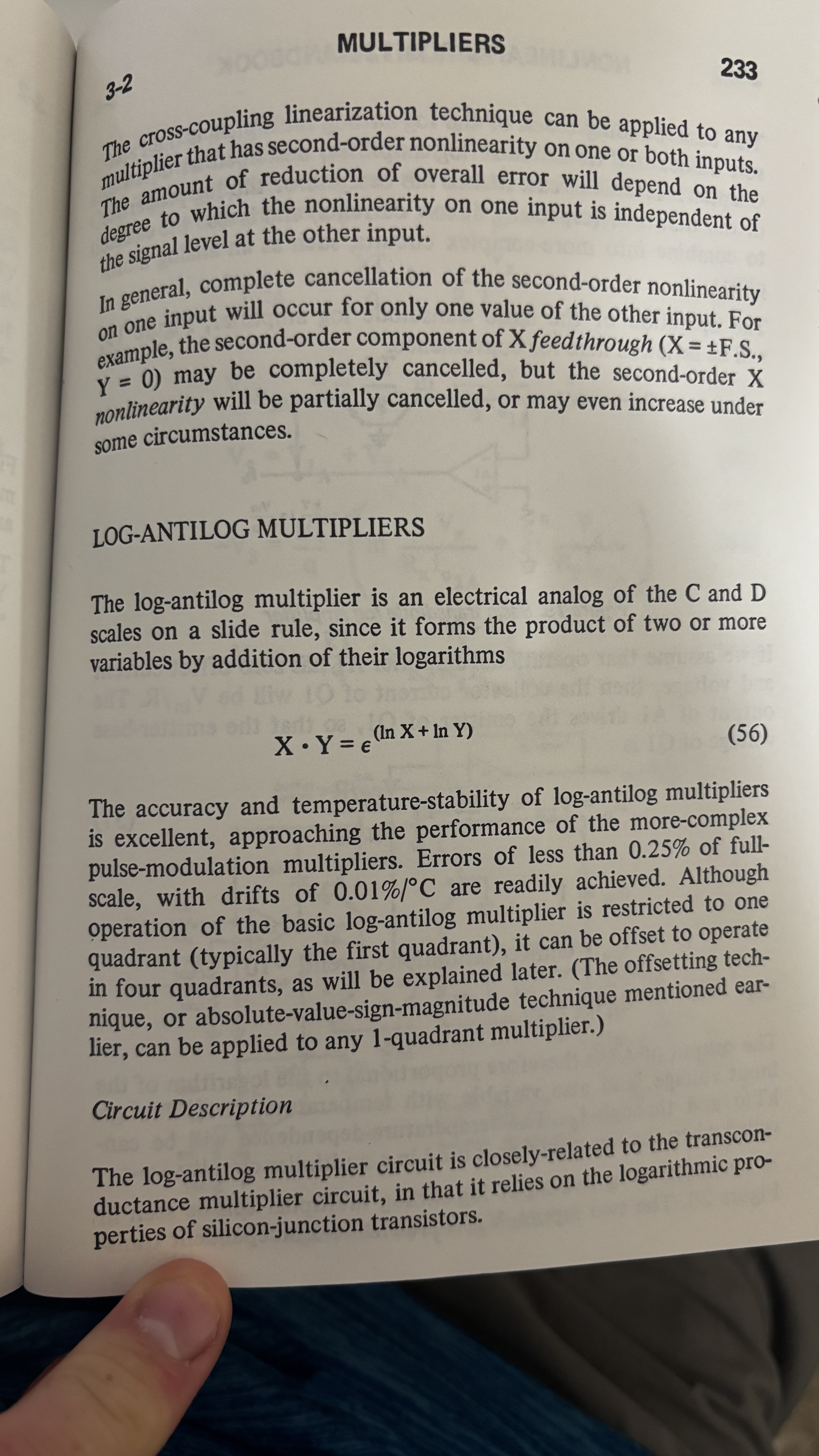
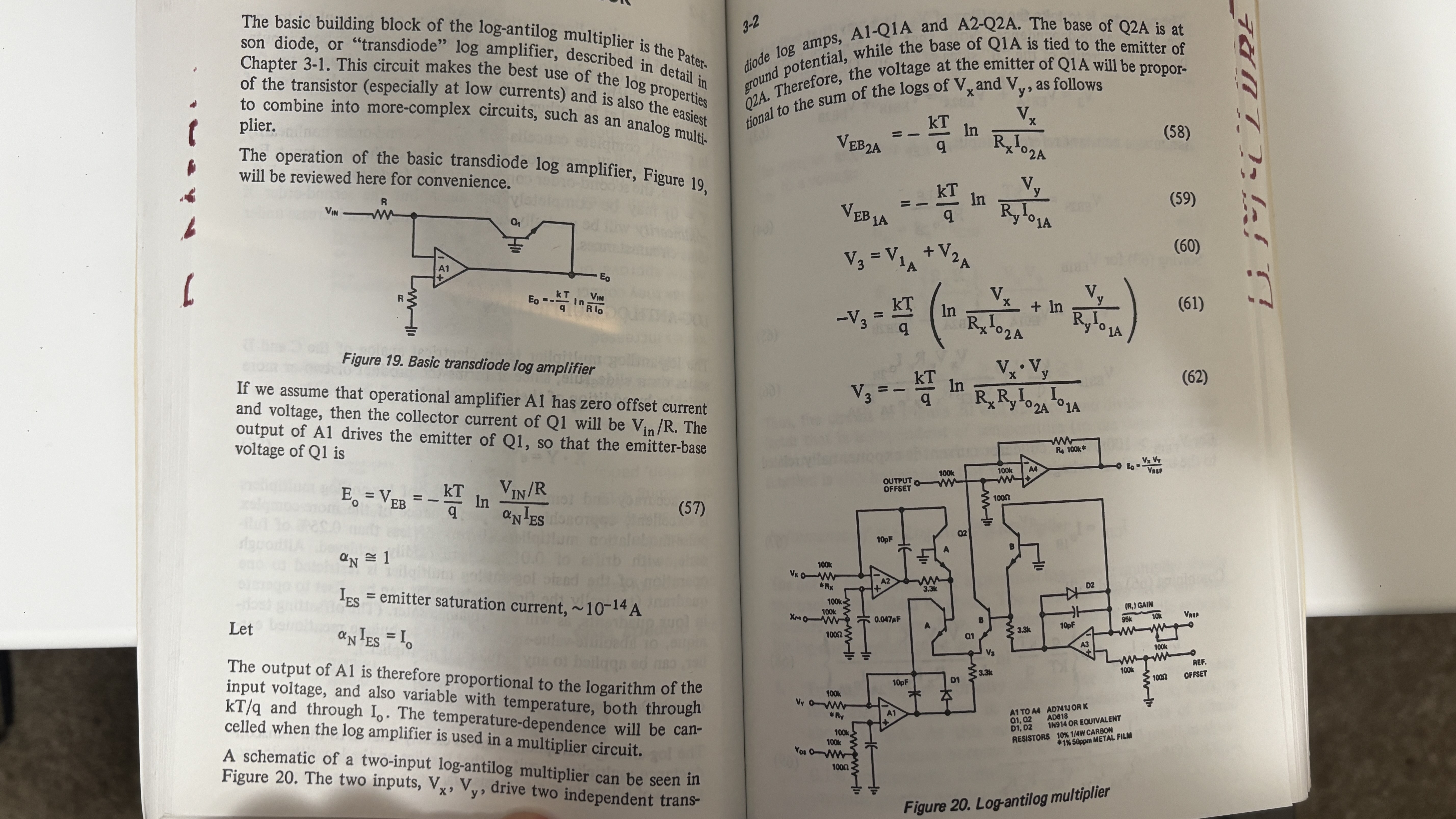
Let’s consider the log-antilog multiplier. While the pages above show everything necessary, I’ll go into simpler and perhaps clearer detail. The basic circuit is
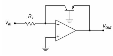
This uses the current flow property of a diode to produce an output voltage. A transistor is just two diodes connected together, (UNDERSTNAD WHY BRIDGE COLLECTOR AND GATE) and if we bridge the collector and gate, we get essentially a single diode but one a lot more stable. So, let’s start with the current flow through a diode:
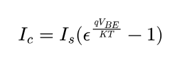
Where $I_c$ is the collector current, $I_s$ is the saturation current (the maximum current that flows when this transistor is switched off), and $V_{BE}$ is the voltage across the base-emitter. There’s a number of constants here ($q$, $K$, $T$), but we know these from physics and can reduce this to
$I_c = I_s(e^{38.6V_{BE}}-1)$
Solving for $V_{BE}$,and noting that the output voltage $V_{out}$ relative to ground is $V_{BE}$
$V_{BE} = C\ln{\frac{I_c}{I_s}}$
Where $C=38.6$. We also know the saturation current of a transistor from the datasheet, and it is $I_s = ~10$ fA. So, vanishingly small, and we can ignore the $C\ln{I_s}$ term. We then have
$\frac{V_{in}}{R_{in}}=I_{in} = e^{V_{out}}$
Therefore $V_{out} = \ln{\frac{V_{in}}{R}}$
Doing a similar trick to the capacitor above when we changed from integrating to differentiating, we move the transistor to the input side instead of feedback loop, and get
$V_{out} = e^{V_{in}}$
If we remember that the sum of logs is the log of the product - $\log{X} + \log{Y} = \log{XY}$ - then we can sum two log-amplifiers and feed the result to an exp op-amp to get
$V_{out} = e^{(\log{V_{in1}} + \log{V_{in2}})}$
So
$V_{out} = V_{in1} \times V_{in2}$
Now there’s a negative in there as well that I’m glossing over, but this can be handled by a simple inverting voltage follower on the output. The important thing to note about this set up is it does not work with negative inputs! (logarithms don’t operate on negatives)
How then, can we handle negative input? We have, after all, an oscillating waveform.
An offset.
Consider, for variables $X$ and $Y$ and constants $A$ and $B$, where $|A| > |X|$, $|B| > |Y|$, and $A, B > 0$: $(X+A)(Y+B) = XY + XB + YA + AB$
Since $X$ and $Y$ are time varying signals that have upper and lower bounds, by choosing $A$ and $B$ (as constant voltage sources, drawn from the same master voltage source powering everything), we can guarantee that $X+A>0$ etc. For example, we might know that $X$ varies between +2v and -2v. Set $A$ to 2v, and $X+A$ goes from 0-4v. The same applies to $Y$ and $B$.
Then, on the output, we can easily compute $XB$, as $B$ is constant, $YA$ for the same reason, and $AB$ can come from a constant voltage source. Since the multiplier output is inverted, use an inverting summer, and we have $V_{out} = -(XY + XB + YA + AB) + XB + YA + AB = -XY$ One more inverting voltage follower, and we arrive at $V_{out} = XY$!
Here’s the circuit for a log-antilog multiplier:
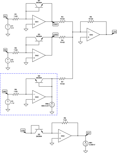
Top left, on OA1 and OA2, we can see two log-amplifiers implemented on V1 and V2. These are summed with an offset voltage across R7, inverted, and then passed to an antilog amplifier below. This offset is just a natural artefact of the components used and we want this to be what the log-antilog system considers “1”, so we pass 1v through a log amplifier.
I made this in simulation and tested it with some generated sine waves of different frequencies, constant values, etc. I like to use small signals so that constants A and B are 1, which just makes the math work nicely: you already have signals X, Y, and 1, and avoid extra scaling and extra voltage sources.
This would cost 5 op-amps to produce (passive components and individual transistors are so cheap their cost is irrelevant), so this is much better than a proper multiplier circuit (op-amps cost ~$1 for one chip containing 4). Here’s my full circuit:
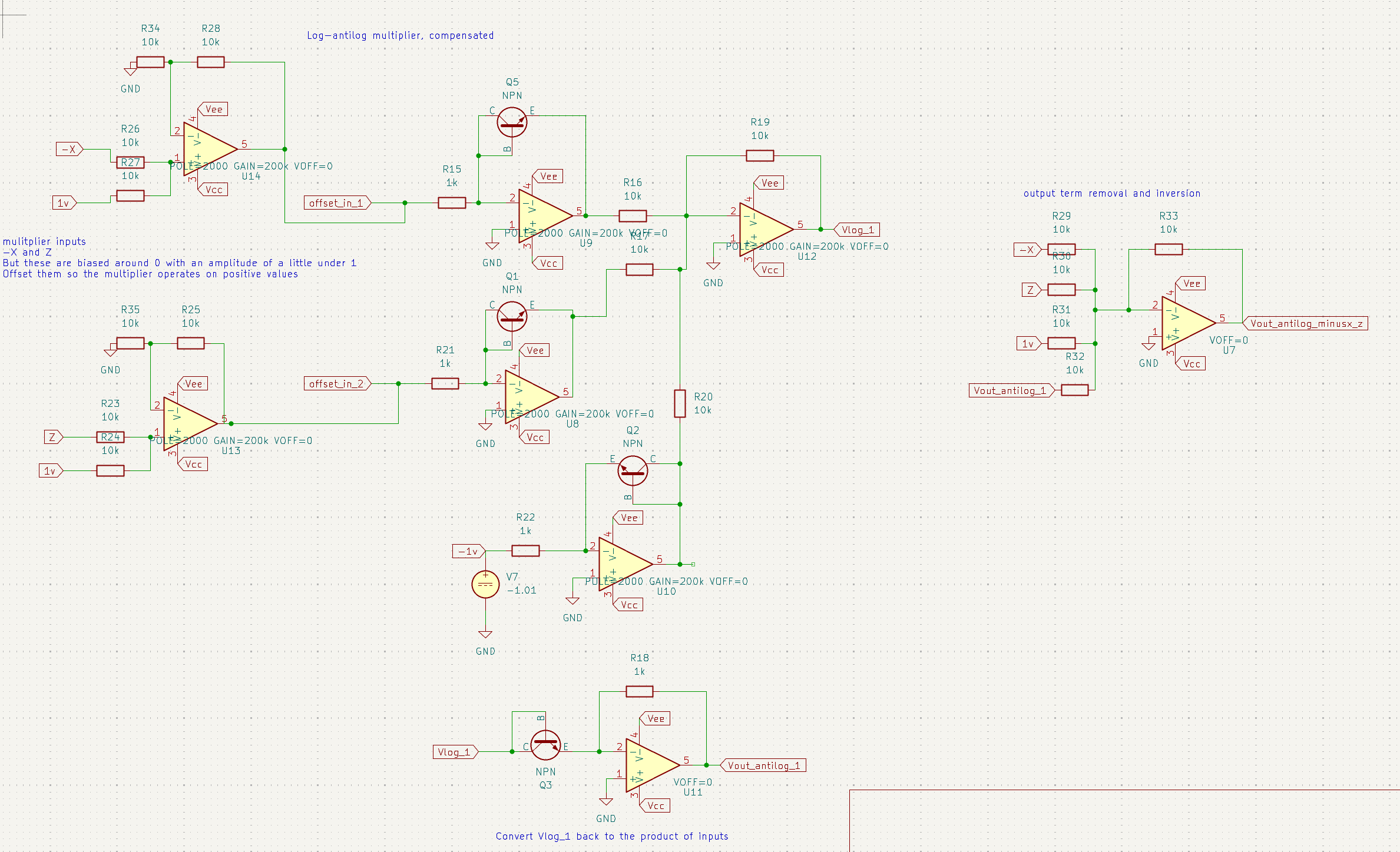
It’s big and complicated, but break down to each op-amp, and the structure should be clear.
Integrating this into the main circuit instead of the ideal voltage sources, we see:
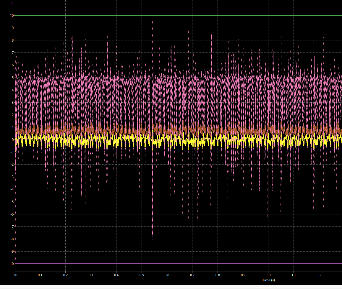
Where Z is pink. Hmm. Let’s run this with the same inputs as the ideal voltage multiplier, and see what’s different:
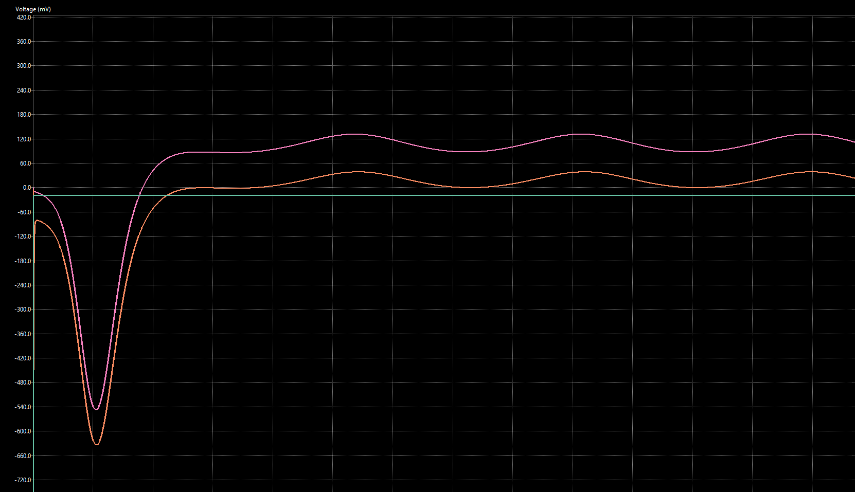
Where pink is the output of the multiplier, and orange is the output of the ideal multiplier (the simulator just multiplied the values it has). The signals are very close! But slightly off, and this causes chaotic effects down the line. This is, after all, a chaotic system of equations. We can try to initialise things nicely, by starting with the ideal product of voltages, and then switching to the designed multiplier after some time:
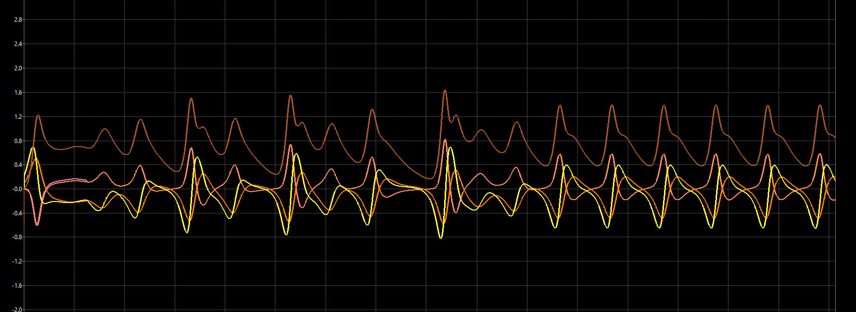
Brown is Z, yellow and orange are Y and X respectively. Pink is simulated source switching to multiplier circuit after some time.
There’s a small jump, unfortunately, but this leads to a stable system at least. I spent considerable time trying to understand this, and didn’t get anywhere. The rabbit hole that digs deep into this would be a considerable time investment
Conclusion
Well, at least I know why multiplier chips are so expensive - they are noise free and avoid small problems like this that translate into larger problems. The delta between ideal and log-antilog multipliers above probably stems from initial conditions and interactions between various simulation models (so says an EE coworker). It’s possible that if I built this circuit physically it would just work and be fine, but if it did not, the debugging would be a herculean effort and better to debug in simulation.
Having said all that, you can now see that there are pieces for all arithmetic in analog circuitry. We can connect a multiplier in a feedback loop with an op-amp and create a divider, by forcing Vout to be one of the inputs, or we can force Vout to be both of the inputs and create a Square Root circuit element. With all these, we can do quite complex mathematics all in analog, and therefore solve all sorts of flow simulations or rocket physics without digital computing. Of course - I’ll reiterate - digital computing is more versatile. But analog is a nice stepping stone.
ended up not building this, as it’s also quite a complex circuit, but it was a fun project to try in simulation, and now I understand multipliers and analog computers considerably better.