SMD components are hard
SMD BGA components are really hard
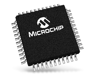
One project I’ve been working on for a while involves circuit board design, and soldering with SMD components. These are - as the acronym goes - Surface Mounted Devices: typically thin, flat pieces that just sit on the circuit board (instead of having pins that go through holes). Their solder pads are usually tinned metal endpoints for things like diodes, capacitors, resistors - all passive components. Active components like microchips vary. These can have little legs that come out and sit on the pad:
Or just flat contacts, so that the capillary action of the solder will connect these and the pad:
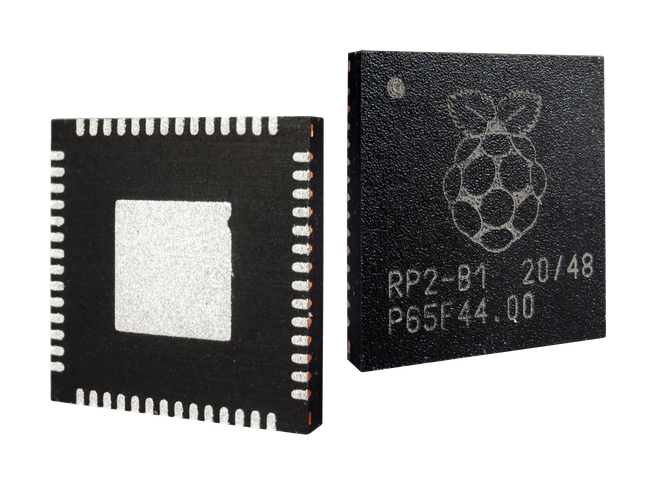
all the way to the most difficult and annoying, and the subject of this post: the Ball Grid Array, which has dots underneath the package:

Why would you do BGA?
BGA allows more pins per surface area. Compare these two again directly:
Some chips, like FPGAs, have just so many output pins it is unrealistic to make a Quad Flat Package (QFP - where it’s got little legs), as the surface area would be increased for just … wires. With multi-layer circuit boards and thin traces (the embedded wires in circuit boards), BGAs aren’t too bad.
So what’s the problem? Soldering them. Namely, how do you know if the pin underneath is properly soldered?
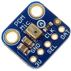
Take a look at this MEMS microphone. This is the pin array underneath. It’s not strictly BGA, but it covers the core concept enough:
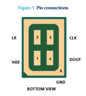
I had one of these soldered down … and it had just soldered on by the GND on one side. Nothing else had soldered. And I had no idea, apart from the circuit working. Another attempt left this:
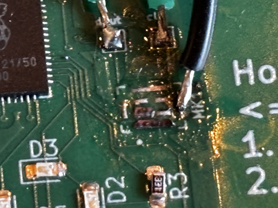
Here you can the GND and one of the pins connected - and tore the contact off - but nothing else did. However, visual inspection showed none of this. How am I going to know?
What can you do?
Ultimately I think the reason this failed is because I used a hot air gun to reflow the circuit. This means that the heat is localised and will heat the outside of the microphone first, before the inside - or perhaps even miss the inside, unless I absolutely cook it. The answer is likely “use a reflow oven”, which is just … an oven. The entire interior is at the required temperature, and the circuit sits in there for a time, so everywhere should reach the necessary temperature. This is how regular BGA chips are soldered, to my knowledge.
Another thing that can be done is reading the datasheet to find advice on how to solder these
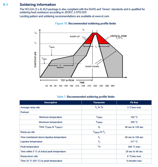
There isn’t much on how to fix it if it’s wrong, but you should follow this advice in the first place.
It should be telling that this advice is at the end rather than the start. I have a habit of “try first, ask questions later”.